
Customer Case
Leak detection of semiconductor ceramic chip packaging
Date:2020-01-06 Views:3605
Reasons for the Need of Leak Detection for Semiconductor Equipment and Materials:
Semiconductor equipment requires high vacuum, such as magnetron sputtering systems, electron beam evaporation systems, ICP (Inductively Coupled Plasma) equipment, PECVD (Plasma-Enhanced Chemical Vapor Deposition) equipment, etc. Leakage will lead to the failure of achieving high vacuum or require a large amount of time, which is time-consuming and labor-intensive.
In a high vacuum environment, the cleanliness is high and there is very little water vapor. Once there is a leak, the dust, suspended particles or debris in the surrounding environment will contaminate the wafers, change the characteristics of the semiconductors and damage their performance. Therefore, helium mass spectrometer leak detection must be carried out during the production process of semiconductor devices.
Some semiconductor equipment uses special gases that are toxic or corrosive. After helium mass spectrometer leak detection, under the condition of a low leakage rate vacuum, these gases are not easy to leak out, and the equipment can promptly pump away the unreacted gases and gaseous reaction products, ensuring the safety of the staff and the atmospheric environment.
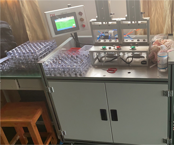
In chip packaging, once there is a leak, the chip will fail.
In conclusion, the helium mass spectrometer leak detector plays a crucial role in the semiconductor industry.
Part of Atlas Copco Group
 Public Security Network Security Record in Anhui Province No. 34010302001915 Product: Helium Mass Spectrometer Leak Detector
Some materials are sourced from the Internet. If there is any infringement, please contact us for deletion.